

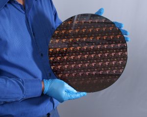
ALBANY, N.Y., May 6, 2021. IBM today unveiled a breakthrough in semiconductor design and process with the development of the world’s first chip announced with 2 nanometer (nm) nanosheet technology.
Semiconductors play critical roles in everything from computing, to appliances, to communication devices, transportation systems, and critical infrastructure.
“The IBM innovation reflected in this new 2 nm chip is essential to the entire semiconductor and IT industry.”
Demand for increased chip performance and energy efficiency continues to rise, especially in the era of hybrid cloud, AI, and the Internet of Things. IBM’s new 2 nm chip technology helps advance the state-of-the-art in the semiconductor industry, addressing this growing demand. It is projected to achieve 45 percent higher performance, or 75 percent lower energy use, than today’s most advanced 7 nm node chips.
The potential benefits of these advanced 2 nm chips could include:
• Quadrupling cell phone battery life, only requiring users to charge their devices every 4 days.
• Slashing the carbon footprint of data centres, which account for 1% of global energy use. Changing all of their servers to 2 nm-based processors could potentially reduce that number significantly.
• Drastically speeding up a laptop’s functions, ranging from quicker processing in applications, to assisting in language translation more easily, to faster internet access.
• Contributing to faster object detection and reaction time in autonomous vehicles like self-driving cars.